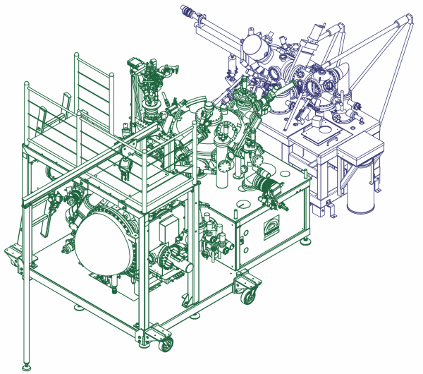
Research modular platform Nanolab consists of several interconnected ultrahigh vacuum modules, including:
a) module of X-ray and Ultraviolet Photoelectron Spectroscopy
Module of ultraviolet and X-ray photoelectron spectroscopy is used for analytical diagnostics of electronic energy and spin structure of synthesized nanosystems with simultaneous correction of details of technological treatment.
Includes:
- UHV chamber with a hemispherical energy analyzer VG Scienta R4000 with microchannel detector and 3D spin Mott detector with a motorized 6-axes manipulator with possibility of cooling by liquid helium, with a narrowband high-intensity UV light source VUV 5k with retractable capillary, with monochromatized X-ray source MX 650;
- UHV chamber for sample preparation completed with equipment for thin film deposition and ion profiling of samples, low-energy electron diffractometer OCI BDL800IR with optics for Auger electron spectroscopy.

Advantages of module of photoelectron spectroscopy:
- Pressure in the analytical chamber during measurements is not higher than 1-2⋅10-10 mbar.
- High energy (<1.8 meV) and angular (<0.1°) resolution of the analyzer.
- Six-axis manipulator Prevac with cooling of sample up to 30 K.
- Flash-machine with heating to a temperature up to 2300 K for atomic surface purity of single crystals of refractory metals.
- Sample synthesis "in situ" by methods of local molecular and atomic epitaxy with control of layer thickness with precision up to parts of monolayer, of atomic layer deposition and chemical assembly.
Extra:
Links to websites of manufacturers PREVAC sp. z o.o. and VG Scienta.
b) module of scanning tunneling and atomic force microscopy
UHV module of scanning tunneling and atomic force microscope with system of imaging technological operations is designed to monitor the results of nanotechnological operations, to study structure of nanoobjects with atomic resolution.
This research platform allows to solve synthesis and diagnostic tasks for nano-objects with description of processes at the atomic level, and analysis of fine features of the electronic energy and spin structure of nano-objects facilitating the creation of cutting-edge technologies and research in the most modern and relevant areas of nanoelectronics (including graphene) and spintronics.
Includes:
- UHV chamber with a scanning probe microscope Omicron VT AFM XA 50/500, allowing the study of the surface structure with atomic resolution in a wide temperature range;
- UHV chamber for sample preparation with equipment for thin film deposition and control their parameters by methods of LEED and Auger spectroscopy.

Advantages of module of scanning tunneling and atomic force microscopy:
- Scanning of the surface of samples with atomic resolution in ultrahigh vacuum (1-2⋅10-10 mbar) conditions.
- Scanning of the sample at temperatures range from 50 to 500 K.
- Modes of a scanning tunneling microscope and atomic force microscope (contact and noncontact modes).
- Possibility of deposition of substances on surface of the sample during the experiment when sample is on the microscope stage.
- The possibility of preparing W tips "in situ" by electron bombardment.
- Sample synthesys by "in situ" methods of local molecular and atomic epitaxy with control of layer thickness with a precision up to parts of a monolayer, of atomic layer deposition and chemical assembly.
Extra:
Link to manufacturer site Omicron NanoTechnology GmbH.


