


- Информация о материале
- Просмотров: 2310
Optical and Quantum Electronics Volume 49, No.1, January 2017, Article 40, Pages 1-9
E. I. Ageev, D. V. Potorochin, D. V. Sachenko, G. V. Odintsova
Generation of web-like structures and nanoparticles by femtosecond laser ablation of silicon target in ambient air
Optical and Quantum Electronics Volume 49, No.1, January 2017, Article 40, Pages 1-9
DOI: 10.1007/s11082-016-0875-5

Silicon nanoparticles were produced by femtosecond laser ablation in ambient air. Obtained samples were studied using dark-field optical microscopy, scanning electron microscopy and Raman-scattering spectroscopy. Two groups of structures can be found: (1) branched amorphous structures with a minimum element size of about 10 nm and incorporations of nanocrystals (0.6–6.6 nm from Raman scattering analysis); (2) larger crystal particles with smooth surface and a typical size of 50–200 nm that provide directional visible light scattering (at dark-field optical microscopy observations). An influence of environment on resulting phase composition of silicon nanoparticles was investigated by numerical evaluation of nanoparticle’s cooling rate. The calculation shows that cooling in ambient air ensures cooling rate sufficient for crystallization.
- Информация о материале
- Просмотров: 2158
Semiconductors Volume 51, No. 1, January 2017, Pages 111–115
D. A. Kudryashov, A. S. Gudovskikh, A. V. Babichev, A. V. Filimonov, A. M. Mozharov, V. F. Agekyan, E. V. Borisov, A. Yu. Serov, and N. G. Filosofov
Nanoscale Cu2O Films: Radio-Frequency Magnetron Sputtering and Structural and Optical Studies
Semiconductors Volume 51, No. 1, January 2017, Pages 111–115
DOI: 10.1134/S1063782617010110
Nanoscale copper (I) oxide layers are formed by magnetron-assisted sputtering onto glassy and silicon substrates in an oxygen-free environment at room temperature, and the structural and optical properties of the layers are studied. It is shown that copper oxide formed on a silicon substrate exhibits a lower degree of disorder than that formed on a glassy substrate, which is supported by the observation of a higher intensity and a smaller half-width of reflections in the diffraction pattern. The highest intensity of reflections in the diffraction pattern is observed for Cu2O films grown on silicon at a magnetron power of 150 W. The absorption and transmittance spectra of these Cu2O films are in agreement with the well-known spectra of bulk crystals. In the Raman spectra of the films, phonons inherent in the crystal lattice of cubic Cu2O crystals are identified.
- Информация о материале
- Просмотров: 2256
Nanotechnology Volume 28, No. 6, January 2017
S. Schlicht, A. Kireev, E. Grachova, S. Tunik, A. Manshina, J. Bachmann
A model electrode of well-defined geometry prepared by direct laser-induced decoration of nanoporous templates with Au–Ag@C nanoparticles
Nanotechnology Volume 28, No. 6, January 2017
DOI: 10.1088/1361-6528/aa536a

We present an original type of model electrode system consisting of bimetallic Au–Ag nanoparticles embedded in an amorphous carbon matrix with an extremely well-defined geometry of parallel, straight, cylindrical macropores. The samples are prepared in one step by direct laser deposition of the metal/carbon composite onto the inner walls of a porous ‘anodic’ alumina matrix serving as a template. The coating is homogeneous from top to bottom of the pores, and the amount of material deposited can be tuned by the duration of the deposition procedure. As a test system, we demonstrate that a bimetallic Ag–Au@C system is catalytically active for the electrochemical oxidation of glucose in alkaline solution, the anodic reaction of a direct glucose fuel cell. Furthermore, the electrocatalytic current density increases with the amount of Ag–Au@C NPs deposited, up to a point at which the pores are clogged with it. This type of model system allows for the systematic study of geometric effects in fuel cell electrodes. It can be generalized to a number of different nanoparticle compositions, and thereby, to various electrocatalytic reactions.
- Информация о материале
- Просмотров: 2232
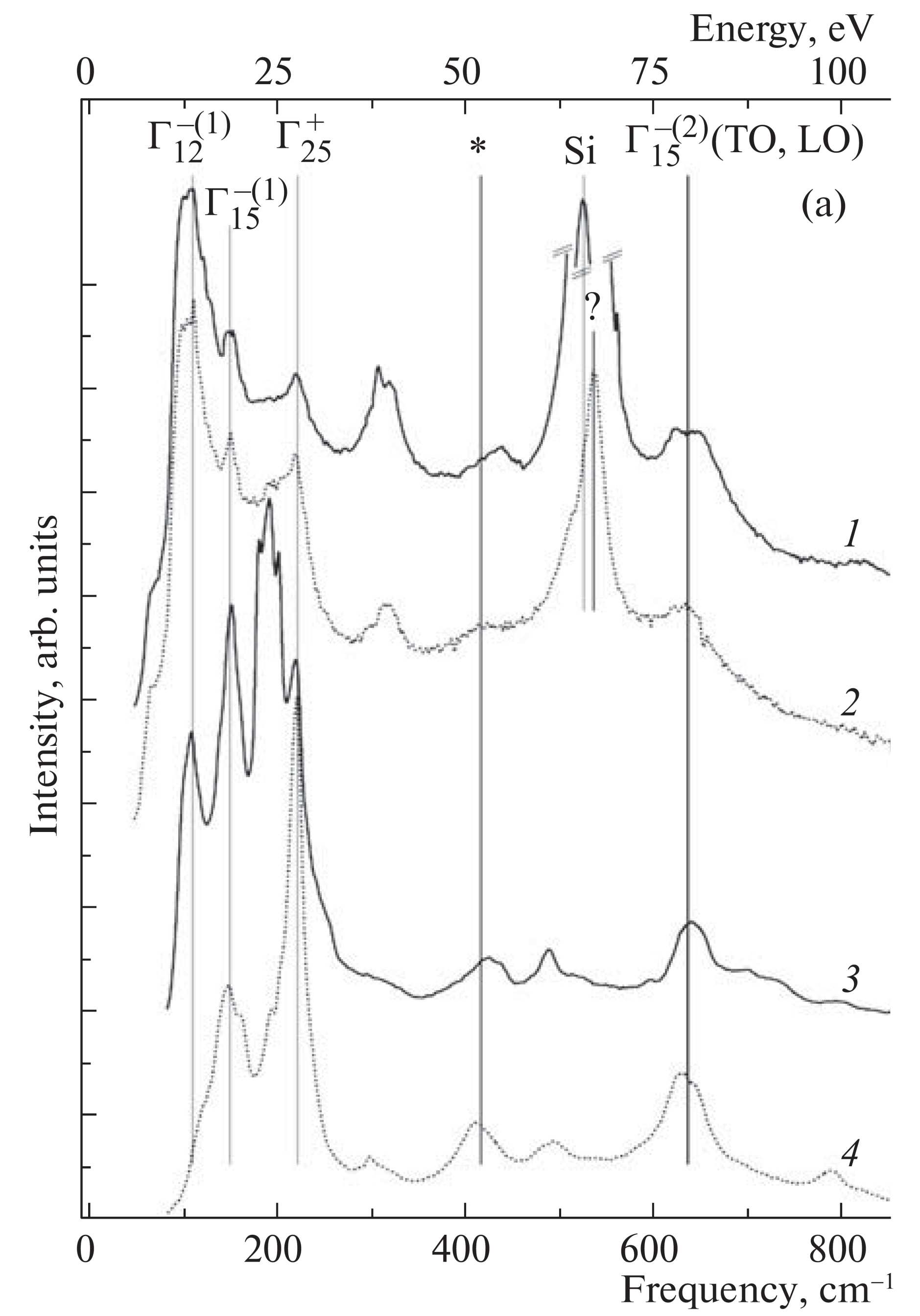
Opt Quant Electron (2017) 49:50
E.I. Ageev, Y.M. Andreeva, P.N. Brunkov, Y. Y. Karlagina, G. V. Odintsova, D.V. Pankin, S.I. Pavlov, V.V. Romanov, R.M. Yatsuk
«Influence of light incident angle on reflectance spectra of metals processed by color laser marking technology»
Opt Quant Electron (2017) 49:50
DOI 10.1007/s11082-016-0876-4

A comparison of oxide films formed on the stainless steel surface during laser and furnace heating is presented. Obtained samples were examined by optical and scanning electron microscopy. In order to characterize the optical properties, reflection spectra within the wavelength range 190–900 nm were measured with a spectrophotometer equipped with the integrating sphere for incidence angles from 0 to 60. The topology of obtained oxide films was characterized by scanning probe microscopy. Due to light interference in produced films, the coloration of treated area is observed. It was found that there is no change in the characteristic appearance of reflectance spectra at different light incidence angles, but a blue-shift occurs especially for the case of laser-induced films, which results in a visible change of surface color. This effect is associated with an interference character of originating color and features of surface relief under an oxide film.
- Информация о материале
- Просмотров: 1641
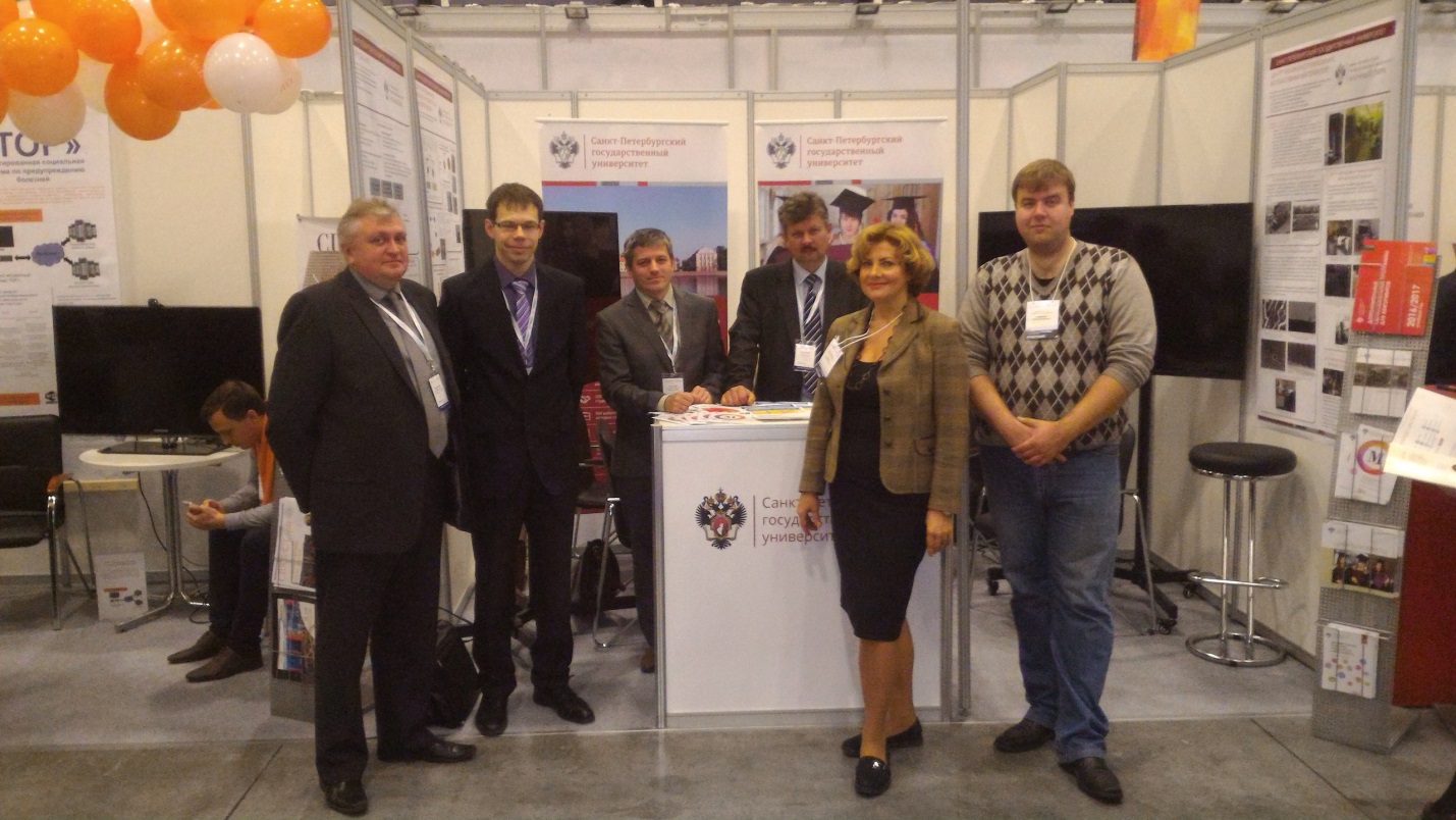
Директор РЦ ОЛМИВ Алексей Викторович Курочкин в составе официальной делегации от Научного Парка СПбГУ принял участие в крупнейшем конгрессно-выставочном мероприятии Северо-Запада, Петербургском международном инновационном форуме.
Университет представил на форуме стенд с информацией о научной инфраструктуре, а также исследованиях и разработках, ведущихся в СПбГУ. В рамках форума представители органов власти, бизнес-структур, а также эксперты высшей школы обсудили актуальные вопросы внедрения инноваций на производстве.
- 20.09.2016 Лаборатория комбинационного рассеяния света РЦ ОЛМИВ пополнилась рамановским спектрометром Horiba Jobin-Yvon LabRam HR800
- 12.09.2016 Ввод в эксплуатацию спектрофотометра Shimadzu UV-3600 для работы в УФ, видимом и ближнем ИК-диапазоне спектра
- 01.09.2016 Ввод в эксплуатацию ИК-Фурье спектрометра Shimadzu IRPrestige-21
- 20.04.2016 Визуализирующая элипсометрия.
- 11.04.2016 Приглашаем Вас посетить семинар «Спектральная визуализирующая эллипсометрия в решении современных научных задач»

")