Semiconductors Volume 51, No. 1, January 2017, Pages 111–115
D. A. Kudryashov, A. S. Gudovskikh, A. V. Babichev, A. V. Filimonov, A. M. Mozharov, V. F. Agekyan, E. V. Borisov, A. Yu. Serov, and N. G. Filosofov
Nanoscale Cu2O Films: Radio-Frequency Magnetron Sputtering and Structural and Optical Studies
Semiconductors Volume 51, No. 1, January 2017, Pages 111–115
DOI: 10.1134/S1063782617010110

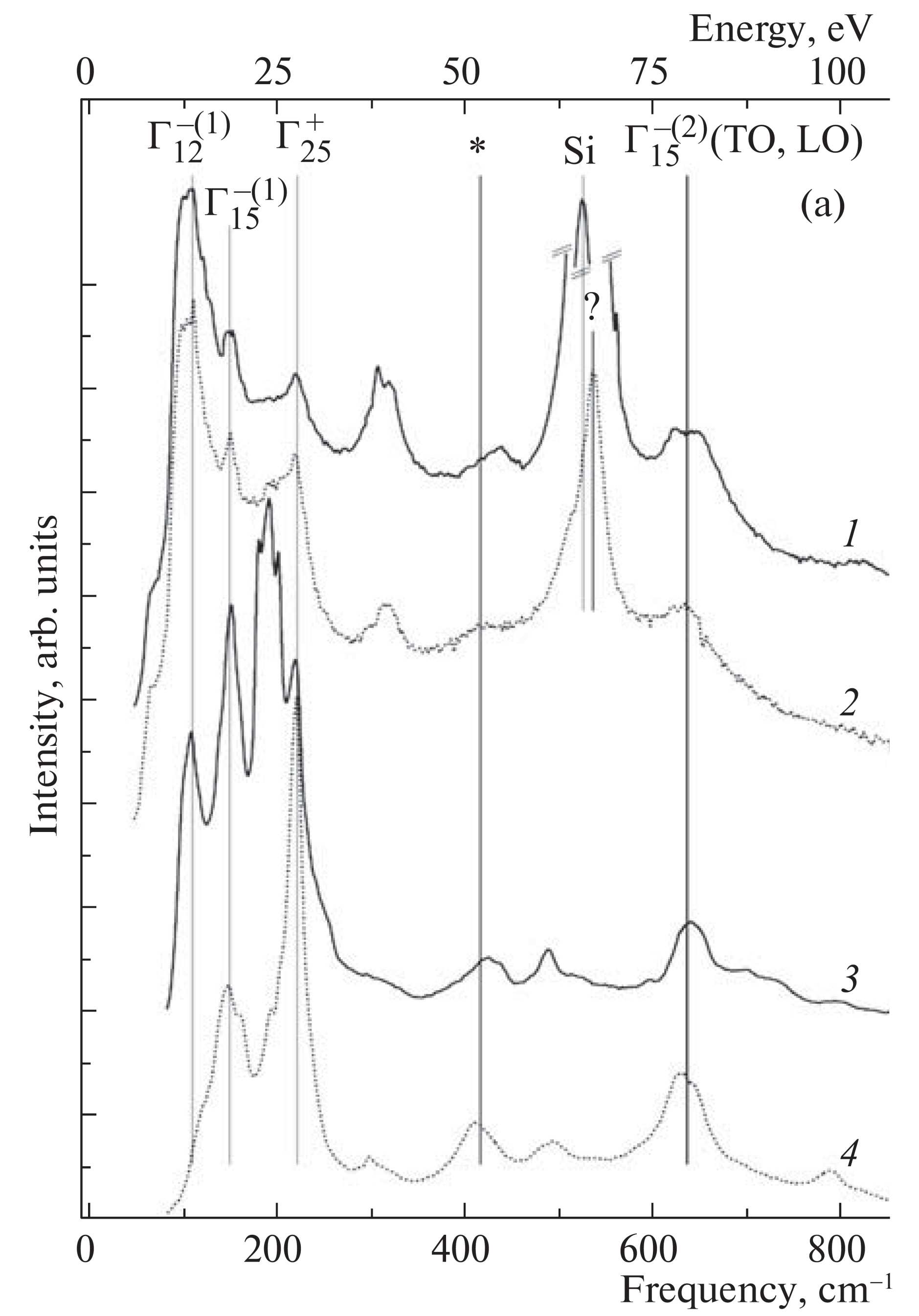
Nanoscale copper (I) oxide layers are formed by magnetron-assisted sputtering onto glassy and silicon substrates in an oxygen-free environment at room temperature, and the structural and optical properties of the layers are studied. It is shown that copper oxide formed on a silicon substrate exhibits a lower degree of disorder than that formed on a glassy substrate, which is supported by the observation of a higher intensity and a smaller half-width of reflections in the diffraction pattern. The highest intensity of reflections in the diffraction pattern is observed for Cu2O films grown on silicon at a magnetron power of 150 W. The absorption and transmittance spectra of these Cu2O films are in agreement with the well-known spectra of bulk crystals. In the Raman spectra of the films, phonons inherent in the crystal lattice of cubic Cu2O crystals are identified.


