

Scanning Helium Ion Microscope is a novel device that incorporate both Focused Ion Beam and Scanning Electron Mycroscopy approaches. Being a very surface tool due to the origin of ion beam with solid interaction it is also the first scanning microscope with a subnanometer resolution (theoretical resolution limit is 0.25 nm) .
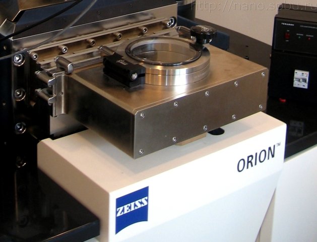


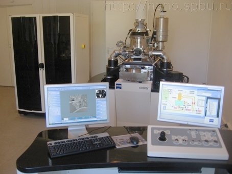
Scanning ion helium microscope Zeiss ORION
Low beam convergence provides high focus depth.
Helium ion beam shows very little diffraction influence because of He ions mass. Since the helium ion beam is much less affected by diffraction, than the electron beam, it can be focused to a smaller probe, enabling sub-nanometer resolution. Features of ions scattering result in high material contrast.
Another feature of helium ion microscope is low beam current, three orders of magnitude lower than typical SEM beam current. It allows to prevent destruction of sample caused by ion beam and to reduce charging of non-conductive specimen surface.
Flood gun charge compensation system allows to work with insulator samples without resolution deterioration.
Parameters of scanning ion microscope Zeiss ORION
Acceleration voltage – 10-40 kV.
Ion beam current – 0.1-100 pA.
Sharpness edge resolution – 0.6 nm.
Backscattered ions detector.
Ion source is tungsten tip which field ionithation of helium atoms takes place on. Scanning field ion microscopy mode allows to observe sourse with atomic resolution to form a trimer and to adjust it mechanically. One of trimers atoms (in the centre of frame) is used as source for beam formation.
Backscattered ions detection (right image) allows to get high material contrast and to observe grains orientation.
Low beam convergence provides high focus depth, higher than typical SEM focus depth.
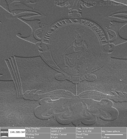
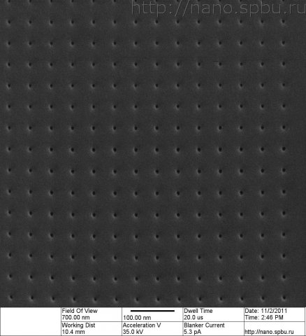
Images, obtained in IRC for Nanotechnology.
NanoMaker lithography system

NanoMaker is a software / hardware system from Interface Ltd. for SEM/FIB based lithography.
System allows performing ion beam lithography, ion beam milling and image aquisition and compensates static distortion and dynamic delays of deflecting system.


")