Studies of surfaces and interfaces between substrates and thin epitaxial layers in both simple and complex multilayer systems. Determination of layer thickness and interface roughness, lattice mismatch and relaxation, composition of solid solution, crystallinity, mosaicity and strain, dislocation density and precise lattice constant measurement. Non-destructive control of bulky industrial single crystals produced for electronics and optical devices. Study of residual stress and textures in ceramic and metallic samples. Microstructural analysis ("size and starin") in both bulky samples and tiny catalyst nanoparticles.
The system includes the following hardware:
LYNXEYE position sensitive 1D (also working in 0D mode) detector for collection of a large quantity of information in a small amount of time plus point scintillation detector for high-resolution measurements.
Centric 1/4-Circle Eulerian Cradle
Sample positioning: motorized Psi(tilt) and Phi(rotation) rotations and X-Y-Z translations. The cradle accommodates bulky specimens (weighing up to 1 kg), powders, thin-films, and wafers.
Laser/video Sample alignment System:
Computer controlled video camera and laser pointer for easy and accurate sample positioning and system alignment.
Goebel Mirror
A parabolic, laterally graded multilayer mirror which converts the divergent beam projected by the line focus of an X-ray tube into a high intensity quasi-monochromatic and highly parallel beam with divergence of 0.03°. White radiation and K lines are eliminated.
2-bounce and 4-bounce Ge crystal monochromators
Using the Gobel mirror as a beam conditioner, the channel cut 2- and 4-bounce Germanium monochromators yields extremely parallel monochromatic (only Cu Ka1) beam with divergence below 0.007° for high resolution applications.
Fine Tilt stage
Motorized tilt stage with a precise knife-edge collimator allows tilting of a sample around 2 perpendicular axes for orientation of sample normal to coincide with the Phi-circle of the Eulerian cradle.
Dual Beam Path analyzer module (PATHFINDER)
Motorized module that allows software controlled switching between 2 diffracted-beam configurations. The first is a high intensity path incorporating a motorized slit, and the second is a high-resolution path incorporating a 3-bounce channel-cut Ge monochromator.
The system can be reconfigured for the following applications:
Grazing Incidence In-Plane XRD (GIIXD)
In-plane diffraction is a technique for measuring the crystal planes that are oriented perpendicular to the surface. As a result, the in-plane lattice parameters and crystal orientation can be determined.
Grazing Incidence XRD (GIXD)
Enhance diffracted signal from polycrystalline thin films and examine structural variations as a function of depth by precisely controlling incident angle and therefore the penetration depth of X-rays.
X-Ray Reflectivity (XRR)
Measures film thickness, roughness (interface and surface), and density of films (1 nm – 1000 nm). Also measures multilayer interface quality and periodicity.
High-Resolution XRD (HRXRD)
Measurement of Rocking Curves is a method for analyzing epitaxial structures with the layer and substrate being almost perfect single crystals. In such a case the difference in diffraction angle for the layer and substrate can be very small and require the capability of resolving Bragg peaks on an arc second scale. The data is recorded as a rocking curve and can be modeled and fitted using sophisticated software to reveal structural details of the epitaxial layers.
Reciprocal Space Maps can be recorded for analyzing epitaxial (and similar) thin films. Narrow scans of reciprocal lattice points are performed for various diffractometer settings and the scattered intensity can be plotted in a 2-dimensional frame.
Texture (pole figures)
A pole figure is measured at a fixed scattering angle (constant d spacing) and consists of a series of Phi-scans (in-plane rotation around the center of the sample) at different tilt or Psi angles and measures preferred crystallite orientation. Measurement times are much faster when using a 2D area detector.
Residual stress
Stress is determined by recording the angular shift of a given Bragg reflection as a function of sample tilt (Psi). This actually provides a measure of strain in the sample from which the stress can then be calculated by plotting the change in d-spacing against sin2psi. This measurement is faster and more accurate when calculations are based on the distortion of the entire Debye ring which is possible when using a 2D area detector.
Microdiffraction and capillary diffraction
Small sample amounts, and/or samples which tend to have texture can be prepared in thin glass capillaries; wires and fibres can also be measured in a similar way. A fast, reliable diffraction pattern can be acquired when the signal is detected over a large portion of the solid angle with an area detector. Small areas on larger samples can be probed using this method with the laser/video sample alignment and sample positioning of the Eulerian cradle.
Traditional powder diffractograms can also be recorded using the parallel-beam geometry. Profile analysis of diffraction peaks or wide-angle full profile analysis allows determination of microstrain and crystallite size and size distribution function. Those can either be directly related to grain size or be different due to presence of defects. This allows characterization of defect-induced substructure.
The Figure 1 below illustrates the evolution of the diffraction pattern of an industrial methanol synthesis catalyst. The dotted line represents the fresh material, and the full line – the one studied after reaction. Sharpening of the profile is caused by sintering of the Cu particles accompanied with a decrease in planar defect concentration. Presence of such defects was shown to be a principal factor for high catalytic activity.
The Figure 2 shows a diffraction curve, and Figure 3 – a reflectometry XRR scan of a semiconductor multilayer sample.

Figure 1.
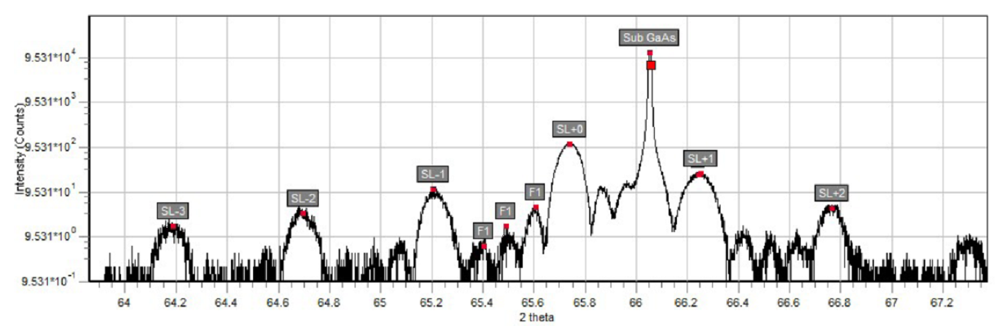
Figure 2. Theta-2theta scan of a semiconductor multilayer sample
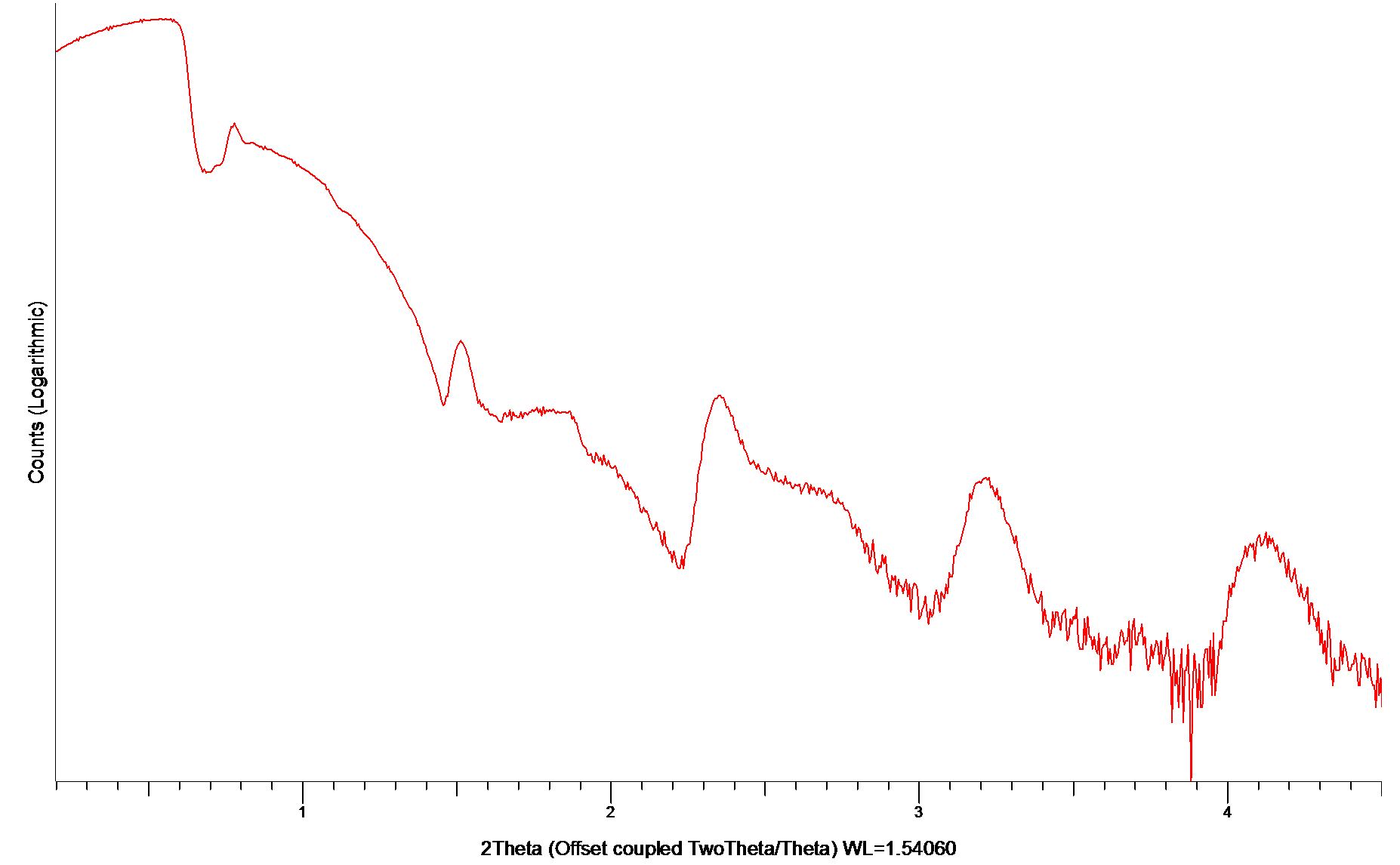
Figure 3. Reflectometry scan of a semiconductor multilayer sample
Equipment
• The research facility Bruker "D8 DISCOVER"
Contacts
• Igor Kasatkin The Leading Researcher in X-Ray diffraction defectoscopy